Getting started with KiCAD
KiCAD is an open-source software to design printed circuit boards (PCB). The documentation exists but is spread around forum posts and difficult to find. Even official contributors admit that the documentation is in a bad state. In this article I describe how to create a very simple PCB based on a BuildElectronicCircuits video.
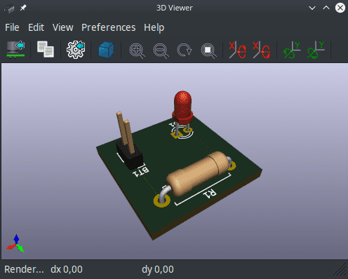
Here is what we will create:
Installation on Linux
The installation process documentation is decent, just follow the instructions for you system on the download page. I'll be using the 5.1.5 stable release.
Setting up librairies
KiCAD can create schematics and PCB layouts. That means we will be manipulating symbols and footprints. KiCAD generally comes preinstalled with a library of symbols and footprints but there are other libraries around that we can import.
In this section we will import the Digi-Key library in a very straightforward way, if you need to know all the internals read this forum post.
Directory structure
Let's create the directory where our library will be stored.
mkdir -p ~/KiCAD/LibDownloading the library
We download the Digi-Key library :
cd ~/KiCAD/Lib
git clone https://github.com/Digi-Key/digikey-kicad-library
Adding a symbol library in KiCAD
- Open KiCAD.
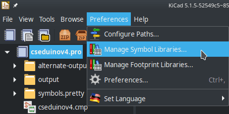
- In the top menu select Preferences > Manage Symbol Libraries....
- A new window appears, select Global Libraries.
- The window has a row of buttons below the table listing all libraries, click on the folder button next to the + button.
- A file browser opens. Navigate to
~/KiCAD/Lib/digikey-kicad-library/digikey-symbols. - Press
CTRL+Ato select every file and clickOpen. - A bunch of rows starting with
dk_have been added to the table. ClickOKto exit.
The libraries have been imported.
Checking if the import worked
To verify that the library was properly imported, open KiCAD and select the Symbol Editor.
![]()
In the filter search for dk_ if you see something then everything worked.
Adding a footprint library
- Open KiCAD.
- In the top menu select Preferences > Manage Footprint Libraries....
- A new window appears, select Global Libraries.
- The window has a row of buttons below the table listing all libraries, click on the folder button next to the + button.
- A file browser opens. Navigate to
~/KiCAD/Lib/digikey-kicad-library/. - Select every folder ending with
.prettyand clickOK. - A new row named
digikey-footprintshas been added. ClickOKto exit.
Other libraries to import
Here is a list of other interesting libraries you might want to add:
- Sparkfun: https://github.com/sparkfun/SparkFun-KiCad-Libraries
- Digi-Key partners: https://github.com/Digi-Key/digikey-partner-kicad-library
- SnapEDA: https://www.snapeda.com/kicad/ (one by one)
- KiCAD footprints: https://github.com/KiCad/kicad-footprints
- KiCAD symbols: https://github.com/KiCad/kicad-symbols
- KiCAD packages 3D: https://github.com/KiCad/kicad-packages3D
Staying up to date
The advantage of using Github is that we can update the library with a simple git pull.
We can do the same with the official libraries but this means removing the preinstalled library and modifying some path variables.
- Download the KiCAD libraries (footprints, symbols and packages 3D).
- Open KiCAD.
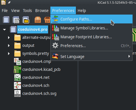
- Select Preferences > Configure Paths
- Set
KICAD_SYMBOL_DIRto~/KiCAD/Lib/kicad-symbolsor wherever you downloaded this library. - Set
KISYS3DMODto~/KiCAD/Lib/kicad-packages3D. - Set
KISYSMODto~/KiCAD/Lib/kicad-footprints.
Creating a schematic
New project
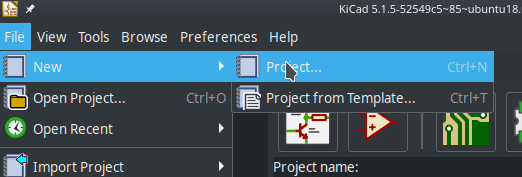
Let's start by creating a new project with File > New > Project... or with the hotkey CTRL + N. I named the project simple-led.
KiCAD automatically creates three files:
- simple-led.kicad_pcb : this stores the info about the PCB
- simple-led.pro : this stores info about the project itself
- simple-led.sch : this stores info about the schematic
We edit the schematic by clicking on the KiCAD Schematic Editor Icon:
![]()
Adding symbols
A new window appears where we can insert our symbols and create the wiring.
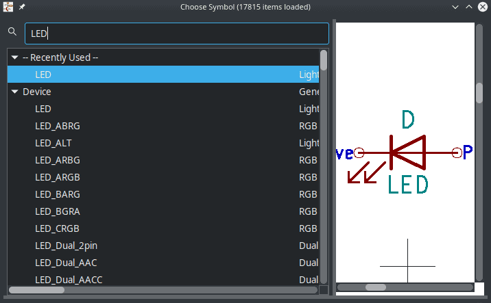
To insert new symbols press A and use the search bar to locate the symbol you are looking for:
If you need to edit a symbol, just right-click on it to display a menu of available actions. Here are some hotkeys that will be very useful when editing a schematic:
- You can move a symbol by hovering it, pressing
Monce and moving it with your mouse. - You can rotate a symbol by hovering it and pressing
R. - You can edit a value by hovering the symbol and pressing
E.
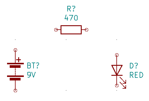
Below I created a schematic with:
- a battery
- a resistor
- a LED
I also set some values (respectively 9V, 470, and "RED").
Adding annotations
To automatically create some annotations select Tools > Annotate schematic and then click on Annotate.
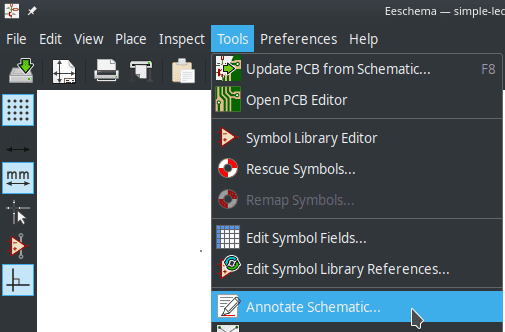
This will automatically add annotations BT1 for the battery, R1 for the resistor and D1 for the LED.
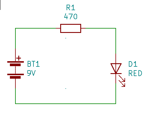
Wiring everything
To wire symbols together place your cursor where the wire should start and press W.
You can left click on the schematic to create "breaks" and turn. The wire stops when you click on the junction of another symbol.
Adding footprints
To add footprints select Tools > Assign footprints.
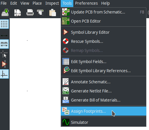
A new window opens where you can select your footprints. The middle column lists the symbols we have added and the footprint assigned to each symbol. Here nothing is assigned yet so the descriptions are empty.
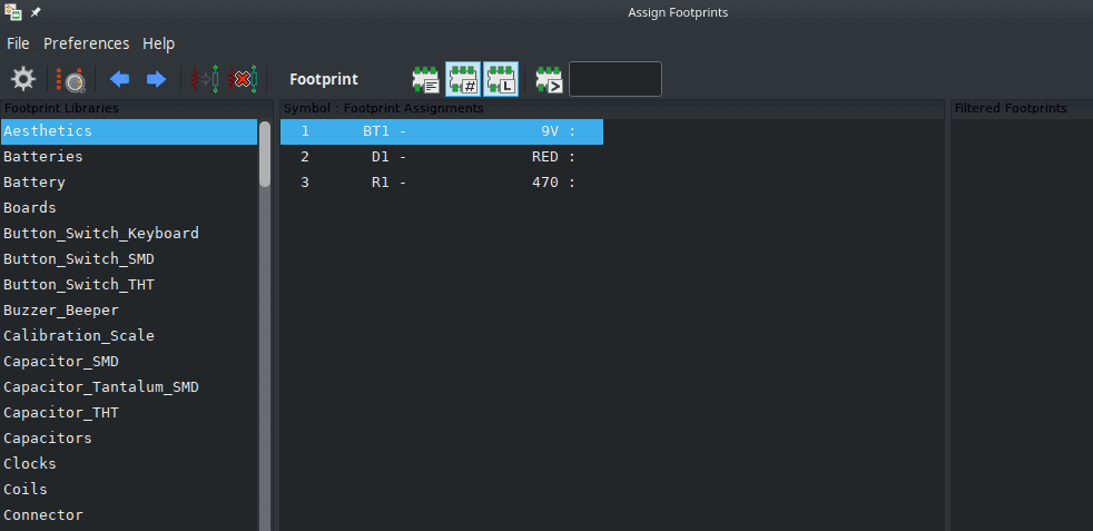
The column on the left titled Footprint Libraries lists the libraries we have imported. If we select one of the libraries the column on the right contains each footprint contained in this library.
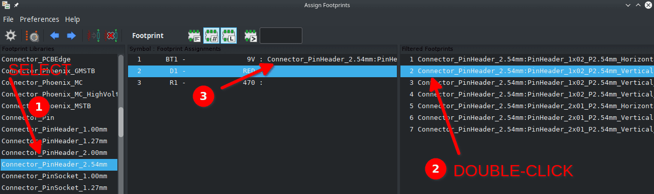
For the battery symbol we will select a header pin.
- We click on the first symbol BT1 to select the battery.
- Then we select the footprint library Connector_PinHeader_2.54mm in the left column.
- Finally we double click on one of the pin headers that are vertical in the right column.
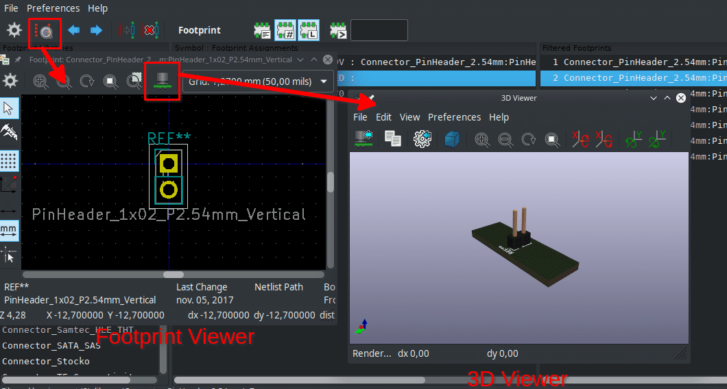
You can preview the footprints with the View selected footprint button next to the gear icon. This opens a new window. On this new window you have the ability to show a 3D preview of the footprint with the 3D Display button (or by pressing ALT + 3):
Here are my footprint associations:
| Symbol | Footprint |
|---|---|
| BT1 | Connector_PinHeader_2.54mm:PinHeader_1x01_P2.54mm_Vertical |
| D1 | LED_THT:LED_D3.0mm |
| R1 | Resistor_THT:R_Axial_DIN0411_L9.9mm_D3.6mm_P12.70mm_Horizontal |
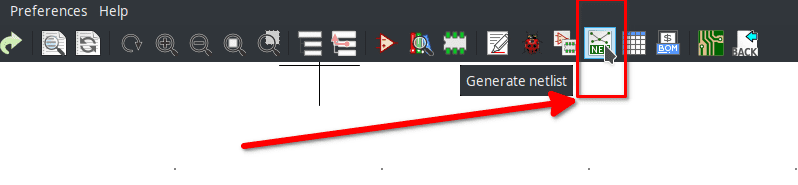
Creating the netlist
To generate a netlist click on the corresponding button in the toolbar. Then in the Pcbnew tab click on Generate Netlist. We save the file as simple-led.net.
PCB
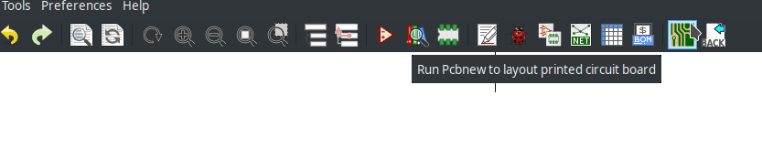
Netlist loading
We are done with our schematic, we can now create our PCB. We click on the button Run pcbnew to layout printed circuit board in the toolbar to open the Pcbnew interface.
In the new window we click on the Load netlist button to load our previously saved netlist.
![]()
We can then select our netlist file and click Update PCB.
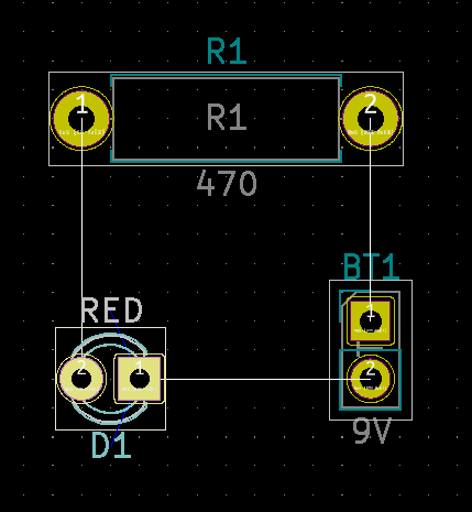
Moving the components
Our components are loaded, we just need to click somewhere to place all of them. The commands are identical to those in the schematic editor, except that you have to click on a component to select it before moving or rotating it.
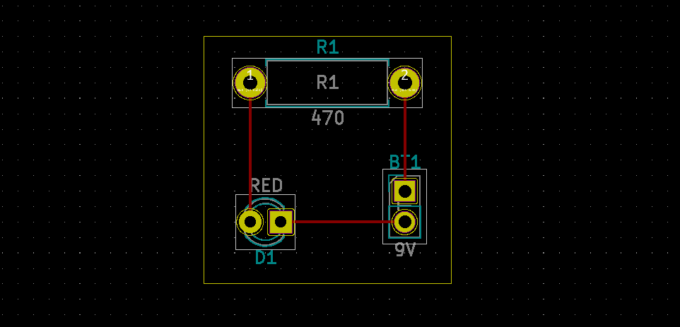
Move and rotate your components to improve their placement and achieve something like this:
Drawing the routes
To draw the connections between each component we use the Route tracks tool on the right side toolbar.
Start by selecting the layer F.Cu which is the Front Copper layer. Then click on the Route tracks tool or press the hotkey X. You can now draw the routes between each components:
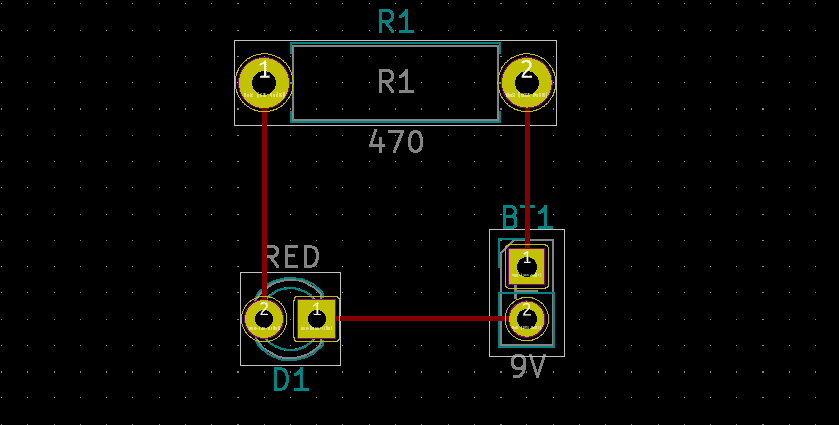
You can select B.Cu to draw wires on the back of the board.
Drawing the board outline
To draw the outline of the board select Edge.Cuts instead of F.Cu and click on the Add graphic lines button. You can now draw a rectangle around your components; use double-click to finish.
3D Viewer
The board is finished, you can display a 3D view with View > 3D Viewer or with the hotkey ALT + 3.
Conclusion
KiCAD is a great open-source and free tool for your electronics projects. I am not an expert in electronics and I am just learning. Seeing that there was no good resource to show how to use KiCAD from start to finish I decided to write this blog article. But this doesn't serve as a documentation. If you want to learn more I highly recommend Digi-Key video tutorials.