From KiCAD to Blender
KiCAD offers a 3D viewer to display our PCB in 3D. It is a great tool but sometimes we want to do more with our 3D view. Maybe we want a beautiful render for our website, or maybe we want to integrate it in a game. This means modifying the 3D model in a software like Blender.
In this article I explain how to use a KiCAD project to create this beautiful 3D PCB render.
As you can see, I am certainly not a Blender professionnal artist, most of the blender related information comes from this video by Jack Humbert. I adapted the material to fit this example.
Exporting the KiCAD project
The KiCAD example project is available on my Github repository
Getting the 3D Model
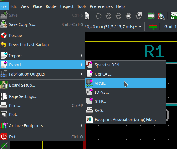
Everything starts with KiCAD. Once we have finished our KiCAD project. We need to export it in VRML format. To do so :
- With your project loaded in KiCAD, open the PCB Layout editor.
- In Pcbnew (the PCB layout editor), select File > Export > VRML....
- Save your file.
Exporting the textures
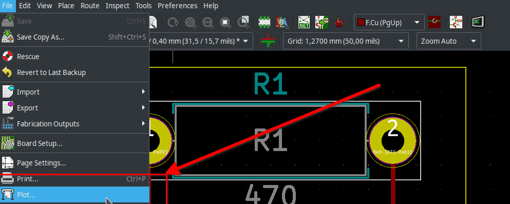
One downside with VRML is that our copper, silk, routes etc. are not included. To be able to use them in blender we need to get each layer as a png file. The closest we can do with Pcbnew is extracting the layers as svg files:
- In Pcbnew select File > Plot....
- Select the plot format to SVG.
- Deselect the Edge.Cuts in the included layers.
- Click on Plot to generate the files
We should have the following files:
- simple-led-B_Cu.svg
- simple-led-B_Mask.svg
- simple-led-B_Paste.svg
- simple-led-B_SilkS.svg
- simple-led-Edge_Cuts.svg
- simple-led-F_Cu.svg
- simple-led-F_Mask.svg
- simple-led-F_Paste.svg
- simple-led-F_SilkS.svg
We just need to convert these svg files to png and we are good to go:
find . -iname '*.svg' -exec bash -c 'inkscape -z -w 2048 -z 2048 "$1" -e $(basename "$1" .svg).png' - '{}' \;Here we use the command inkscape -z -w 2048 -z 2048 input.svg -e output.png
on every svg file.
That's it, we won't need KiCAD anymore in the rest of this article !
Importing the project in Blender
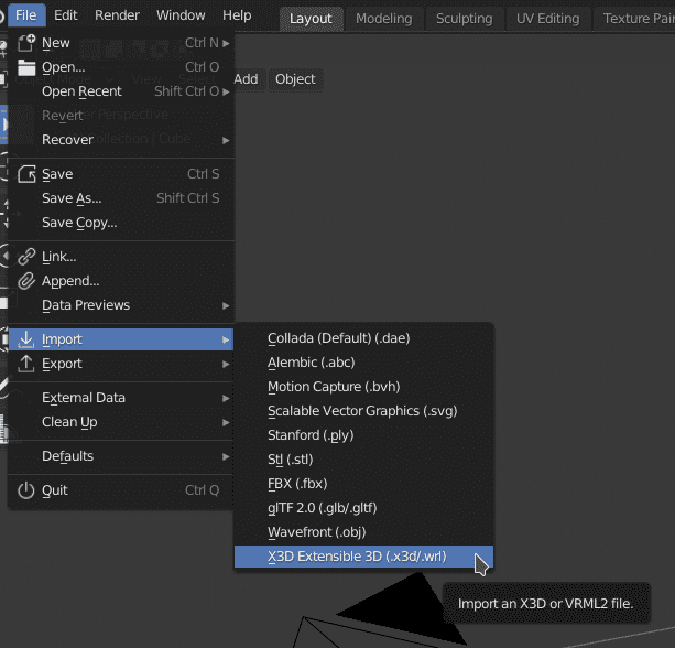
Blender is capable of loading VRML files. To import our previously generated file in Blender select : File > Import > X3D Extensible 3D and then select our VRML file.
Your 3D model is now loaded and you should see a bunch of shapes in the top right hand side corner. If you can't see the model in the 3D view panel, this is is because it is too small. You just need to zoom in to see it properly:
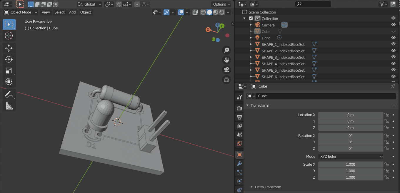
Place the PCB at the center of the viewport. You can use G to move the model and R to rotate it. If you are new to Blender I highly recommend Blender Guru's tutorial they are incredibly well done and fun !
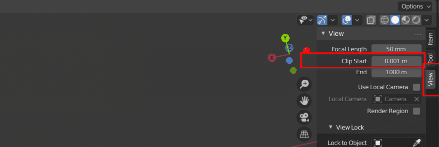
When you try to zoom in on the PCB the object might be cut. This is because the clip start configuration is not adapted. Press N to display the configuration panel and select the tab View. Then set Clip start to the value 0.001m.
Grouping shapes together
Creating collections
As of now, our shapes are in a chaotic state. You might have something like:
- SHAPE_14_IndexedFacedSet
- SHAPE_15_IndexedFacedSet
- SHAPE_16_IndexedFacedSet
This naming is unreadable. To help us work with our 3D model we will group the shapes together according to the component parts. We simply select the shapes we are interested in with the selection tool as shown in the video below. We can remove parts with CTRL + Select and add some with SHIFT + Select. We can also do it manually by selecting the shapes one by one with SHIFT + Left click.
With the shapes selected we press M (or right click and select move to new collection) and move them to a new collection named LED. We can now hide this collection and continue the grouping work.
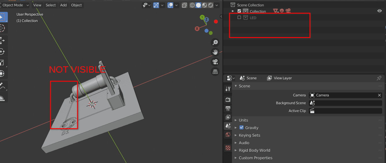
In the end we should be able to create 6 groups:
- Cam/Light
- LED
- PinHeader
- Resistor
- PCB
You might want to add subcollections like LED_head and LED_pins to help working with your model.
Joining objects
Collections are great to quickly separate shapes, but it is better to group them more tightly and merge the meshes. This will allow us to apply materials to one one shape only. Here is how to group every part of the LED head under one object instead of one collection:
- Select one shape constituting the LED head.
- Select all the other shapes of the LED head with
SHIFT + Left click. - Right click in the viewport and select
Join. - Rename the object to
LED_head, move it outside of the collectionLED_headand delete the collection.
Repeat this process for each part made of the same material (plastic, copper, metal, ...). Once this is done we will be able to add shaders to create our plastic and metal textures.
Be careful to separate the PCB soldermask, silk and copper models from the PCB itself as we won't need it. The PCB model should just be the rectangle box with holes. Put the PCB soldermask, silk and copper object in a separate collection that you can turn off easily.
In the rest of the article we will use image files to generate the copper, silk and soldermask directly on the PCB object.
UV mapping the image
In the beginning of the article we saved some .png files. It is time to use them to create the routes and silk.
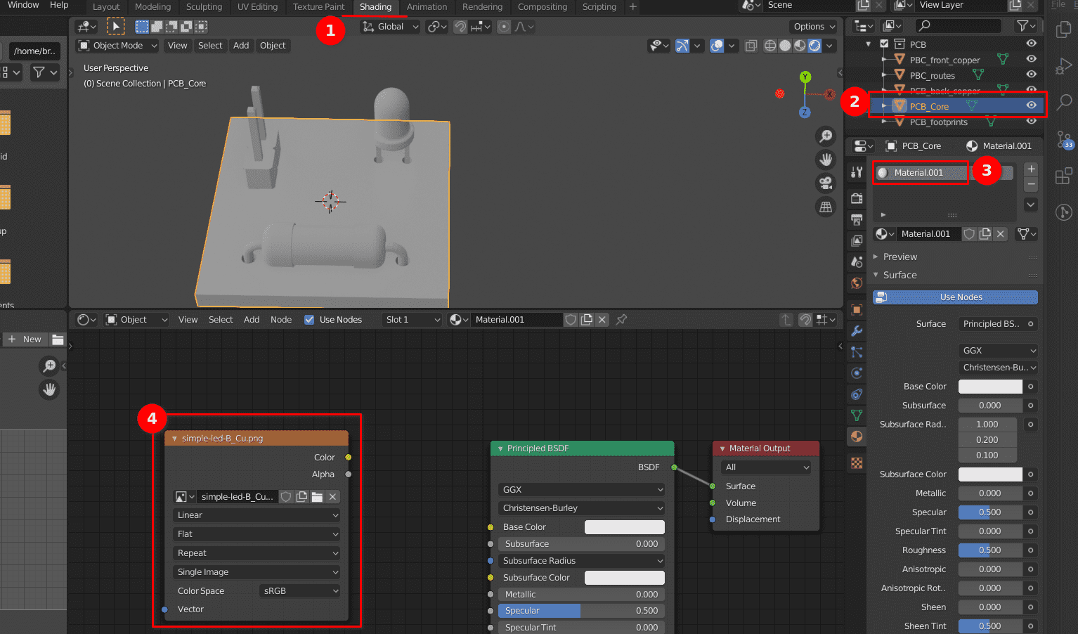
- Go to the Shading view.
- Select the PCB core (the part without the components).
- Add a new material to the object.
- Add a new image texture in the shaders view.
- Import every generated
.pngfile.
The images are loaded, now we need to align them with the 3D model.
- Go to UV Editing.
- Select the PCB core.
- Press
Ato select all. - Press
Uand select Project view (from bounds)
Now in the left box of the UV Editing layout press A to select all and scale and transform the nodes to make it match the loaded png. We might need to rotate or mirror the view from X or Y to make it match. Once this is done we can go back to the Shading editor.
Adding the textures
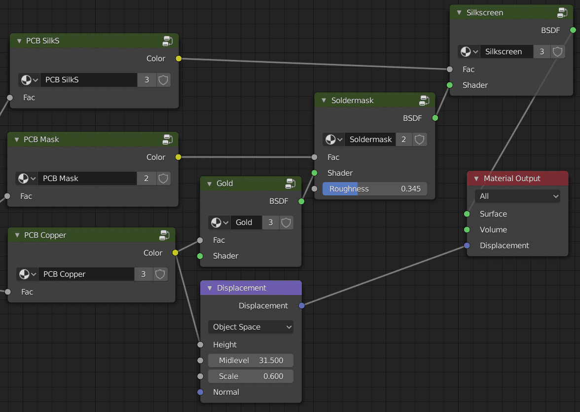
We move on to the Shading editor to add the colors and textures. Before creating anything let's take some time to review what we are set to create. The 3D model of our PCB is going to be structured in multiple layers :
- The first one is the copper layer : we want to fill the PCB holes with copper.
- The second layer is the soldermask : the black protective paint that will come on top. We want to put it everywhere except around the holes. We will invert the copper mask to do so.
- The final layer is the silk for the footprints.
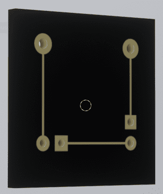
We want to start by adding the layer of copper around and in the holes of the PCB. Like presented in the image below :
In the Shading editor, we add two image textures.
There is one for the top of the PCB (simple-led-F_Cu.png) and one for the bottom of the PCB (simple-led-B_Cu.png). We use a MixRGB shader with a Separate XYZ shader to differentiate between the top and the bottom.
The setup looks like this:
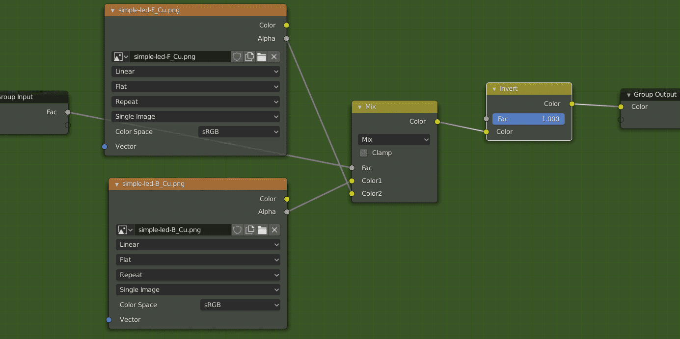
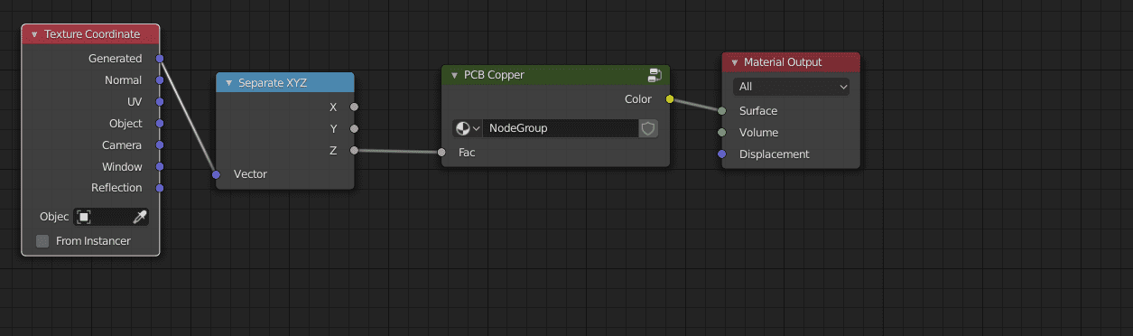
Next we group the image textures and the MixRGB shader by selecting them and pressing the hotkey CTRL + G. We then press TAB to exit the edit mode. We call the group PCB Copper.
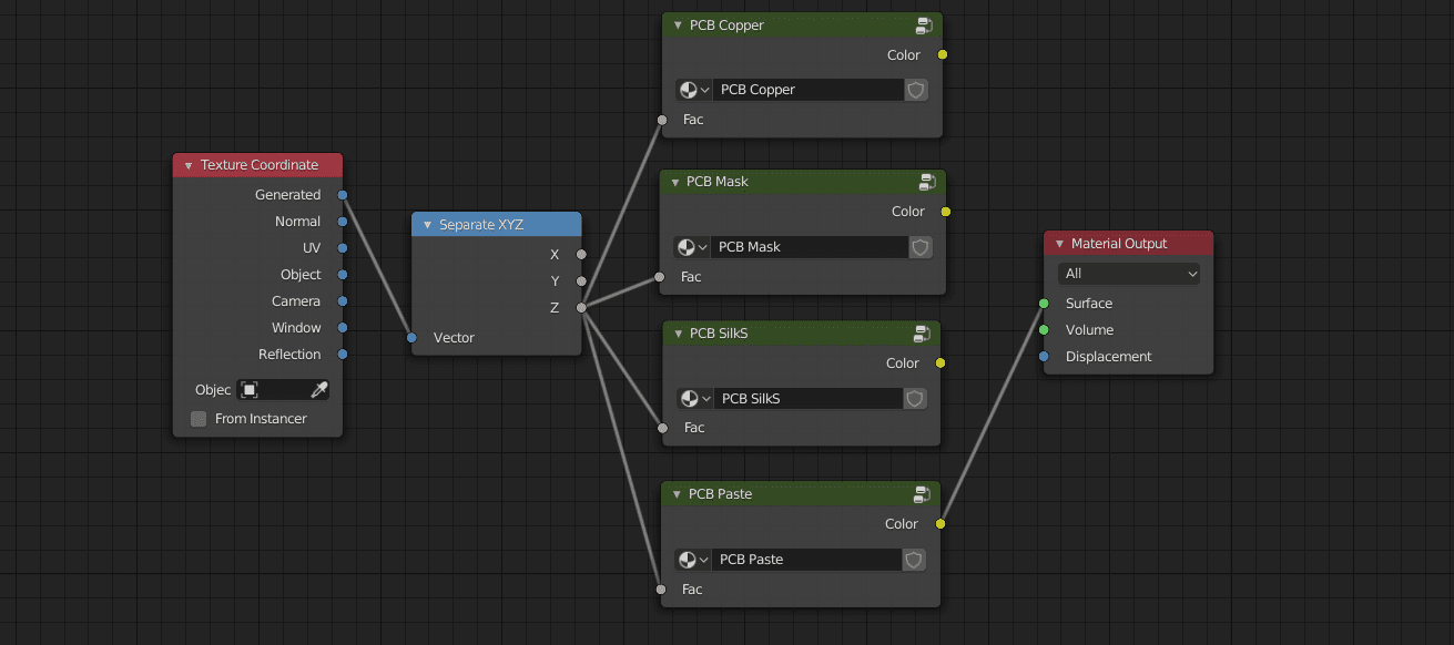
We repeat this process for the mask layer and the silk layer (you can even add in the paste if you have a mask for it).
Adding the metal effects
I'll be using Blender Guru's metal shader to create the Gold and Copper effects.
Check out this stackexchange's answer to learn how to import it.
Once this is imported you should be able to add the Metal Colors shader (SHIFT + A then Group > Metal Colors).
We also create a group IOR-Specular retrieved from blendernation.com which converts IOR to Specular. Note that the formula is given in the Blender official documentation. We can use pixelandpoly to get IOR values.
For instance for Gold, the IOR is 0.470 so we set up the IOR-Specular group accordingly and choose the Gold color in the Metal Colors.
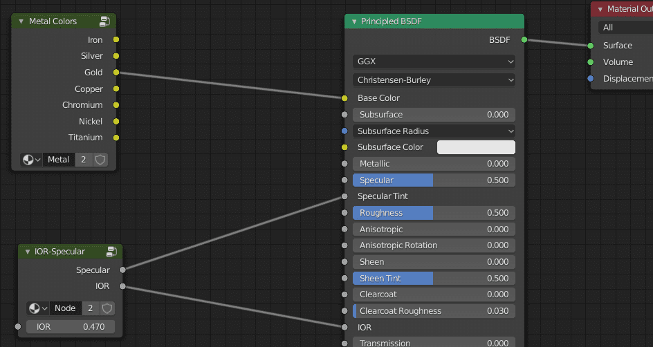
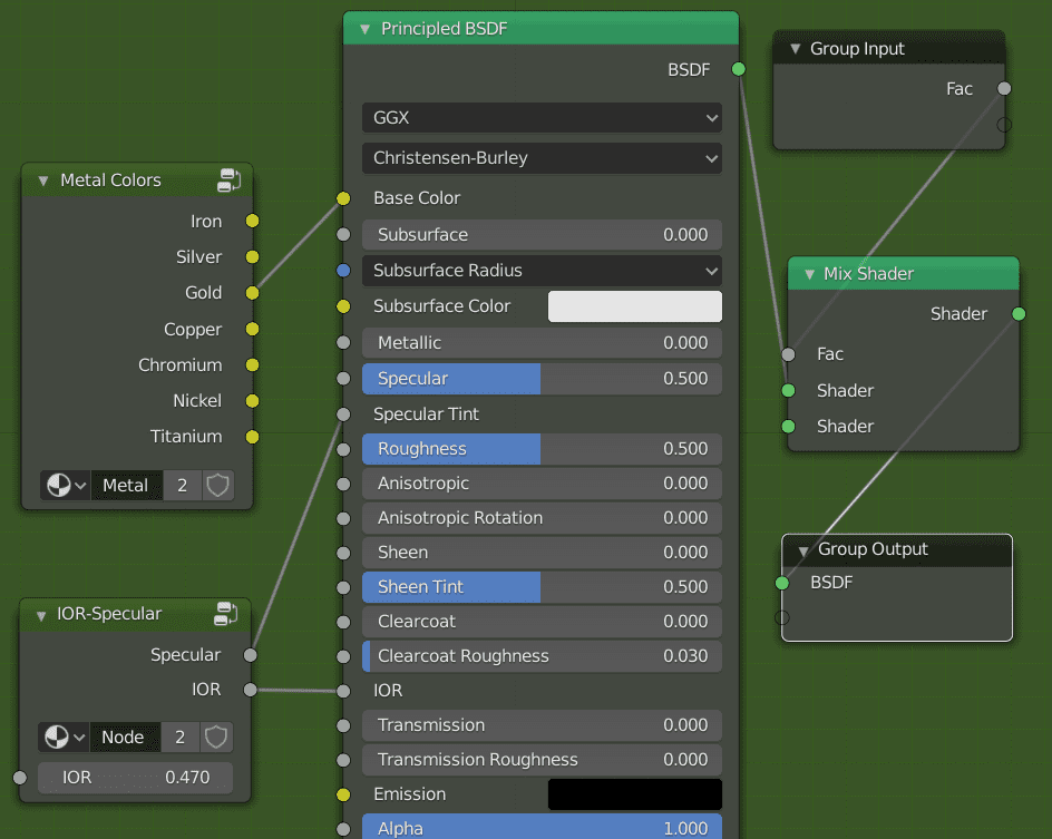
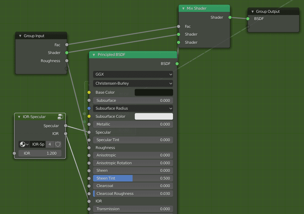
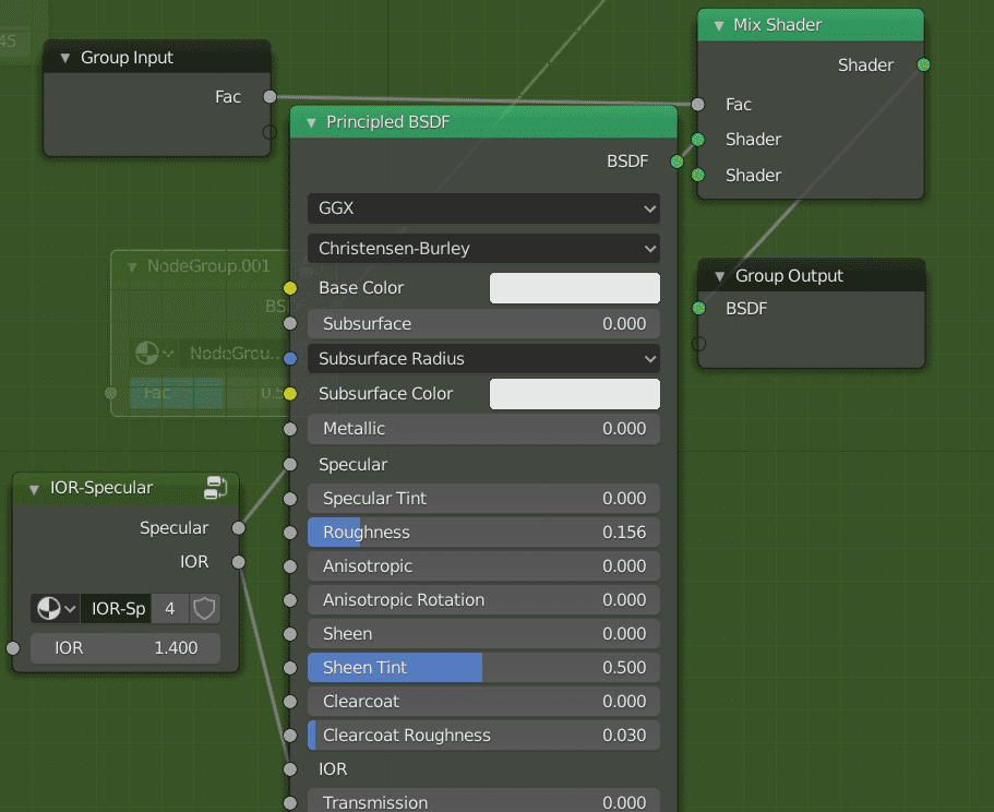
We create a group from the Metal Colors, the IOR-Specular shader and the Principled BSDF named Gold. We can also add a mix shader to ease the use of our Group like shown below.
Next we create a shader for our soldermask and create a group named Soldermask:
We continue with the shader for the silkscreen (we also create a group named Silkscreen):
Once we have our three shaders we just need to link them in the right order :
- At the very bottom sits the copper layer.
- On top of that we add the soldermask.
- And we end with the silk.
We can even add some displacement to create a gap along the copper mask.
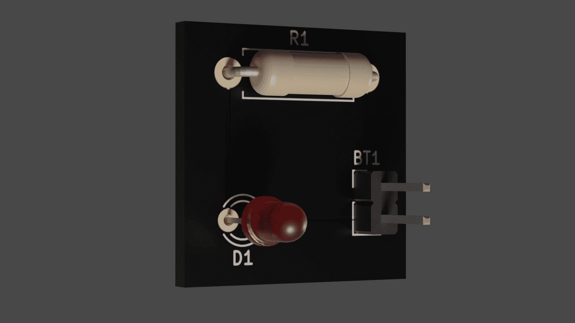
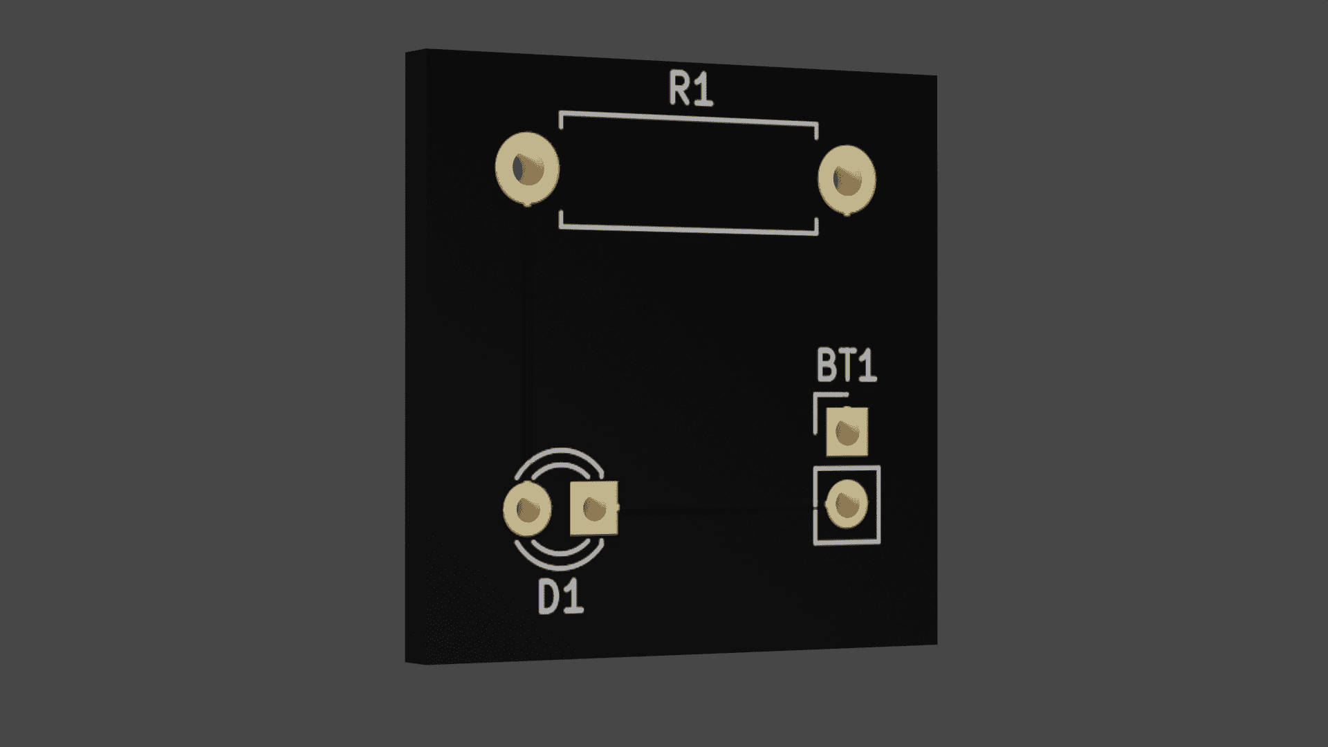
Here is the final result:
Camera view
Here are some tips to work with the camera.
- Select the camera.
- Change the focal length to 100mm.
- Deselect everything with
ALT + A. - Get the view you would like the camera to have (approximately)
- Press
CTRL + ALT + NUM 0: this places the camera at the selected viewport and places us in camera view.
You might not see anything. Select the camera and press G and Z twice to move it along one axis only. You have to move the mouse backward / forward (not the wheel !) to move the camera.
Other components
I'll leave it as an exercise to create the materials for the other components. Here is the final render.
Resources
- Turning a KiCAD design into a realistic render using Blender 2.81
- 'Rendering to Reality: PCB rendering with KiCad, Fusion 360 and Blender' - Greg Davill (KiCon 2019)
- KiCad 5.0 - Importing External 3D Models
- Turntable animaiton with KiCad and Blender
- First Steps - Blender 2.80 Fundamentals
- Blender Guru tutorial
- Led Modeling in Blender